My initial motivation was to build a device that could receive and decode the WWVB time code broadcast from Fort Collins, CO at 60 kHz, and used to synchronize so-called atomic clocks seen on people walls or on their wrists. These clocks really just decode the broadcasts on the WWVB station, which is synchronised to actual atomic clocks co-located with the radio broadcast. The protocol is simple, well understood, and certainly commercial receivers exist, which means a DIY solution has a high likelihood of actually working. The idea here was to build a direct conversion receiver in the style of software defined radio (SDR) on a field programmable gate array (FPGA). This was a great intersection of my interest in FPGAs and SDR, with some mildly practical application, and without having to invest in specialized hardware capable of receiving higher frequencies typical shortwave amateur ratio or FM/AM audio transmissions.
RF receiver theory
There are a lot of ways to encode information in RF waves, and perhaps the easiest to understand is the method employed by WWVB: amplitude modulation. A desired frequency is generated, and simply broadcast at different intensities proportional to the value of some signal. By measuring the change in the intensity of the received broadcast, one can recover a value proportional to the signal. WWVB has two intensities: high and low power, and information is encoded in how long the signal stays in low power mode.
The broadcast signal will propagate as electromagnetic waves emitted from a transmitter antenna, and the electric component of these waves produce a potential gradient along receiver antennas. This potential gradient is measurable at the antenna output as a voltage, which oscillates proportionally to the broadcast frequency. To recover the signal, one must therefore measure the intensity of the oscillations as a function of time. Complicating this problem is the existence of noise and other transmissions at many other frequencies, which will also be picked up by the antenna. Fortunately, there are methods to isolate particular frequencies in arbitrary signals, and other methods to detect the intensities of these frequencies.
Fourier transform into frequency space
Starting from Fourier transforms, it’s pretty obvious how this will work. The measured voltage from the antenna is some function of time , and the Fourier transform of this is
where is now a function of frequency instead of time, and is a complex number whose magnitude is the intensity of the signal at the frequency and phase is the relative phase of that frequency component to the phase of other frequencies.
An aside on complex numbers

For the uninitiated, complex numbers may seem mysterious and unnecessary, but it’s really just a way to combine a magnitude and an angle into a single complex quantity . One could simply keep track of the magnitude and angle, or one could use the more recognized (outside of math and physics) real and imaginary representation, using the “imaginary unit” (or if that makes you less uncomfortable).
Some trigonometry shows that the following expressions hold true.
These expressions are used as the definition of the modulus (or absolute value) and argument (or phase) of the complex number .
The imaginary and real axes representation easily shows that that addition of complex numbers works like vector addition on the complex plane. Less obvious is that multiplication by complex numbers changes magnitude (like multiplication by scalars) but also rotates a complex number on the complex plane. Another way of looking at this is that multiplications scale magnitude and add phases of complex numbers. This is more clear with the more math-friendly representation of complex numbers:
Using Euler’s formula, and a bit of trig, one can see this is equivalent to the above expressions.
With two complex numbers and , multiplication with the magnitude and phase representation clearly shows the scaling of magnitudes and addition of phases.
Back to frequency space
The Fourier transform of the voltage as a function of time gives a function that encodes the magnitude and phase of each frequency in the signal. So, (the magnitude of the complex number) would be the intensity of the received 60 kHz WWVB station within some slice of voltage - exactly what I want.
I’ve suggestively rearranged this into the real and imaginary parts of a complex number, which I take the magnitude of to find the intensity, and everything is a real number again.
I and Q modulation
In the world of RF modulation, the parts being squared above are referred to as the “in-phase” and “quadrature” parts of a signal. For RF, the carrier frequency ( here) is typically much faster than the timescale on which information in the signal (intensity, here) changes. This ends up being critical, since we’re ultimately not interested in the time-averaged intensity but in the intensity as a function of time . A crude way of thinking about this would be to integrate over small slices of time that are long enough to capture many periods of the carrier.
This is effectively describing a low pass filter, which averages over high frequency oscillations to preserve only low frequency components. This is exactly what real radio hardware does to recover information from broadcast signals, first multiplying (mixing) by an oscillating signal at two phases (in-phase and quadrature), and then applying a low-pass filter to the result.
A mixed signal for the in-phase and quadrature parts at some frequency can be defined as:
After applying some low-pass filtering technique, one arrives at the actual and functions used in RF modulation.
The usefulness of this in-phase and quadrature representation, is that (what is broadcast or received) can be generated from and even easier:
Again, this all only works if the time-variation of and is slower than the carrier frequency , such that the low pass technique above is applicable.
Simple amplitude modulation
As a concrete example, the simple case of the WWVB station would use a and an that is one of two values as a function of time, so would be proportional to , where contains the time dependence of the information. Assuming the receiving station is in-phase with the broadcast, the mixed signals would be proportional to:
Applying trig product rules results in:
So there’s an oscillatory part at twice the carrier frequency, and a constant part proportional to . Applying low pass filtering to remove the high frequency part yields something proportional to:
Or, exactly the information that the station broadcast! If there were a phase difference between the receiving and broadcast stations, or one of the stations were moving, part of would be in-phase, and part quadrature. A bit of math would show that would be proportional to what the station broadcast, regardless of phase difference.
State-of-the-art modulation
I won’t be using it here, since the WWVB broadcast is not state-of-the-art, but I/Q modulation underpins all forms of modern long range data transmission, from telephone/cable modems to wifi transmission to fiber optical signals to deep space communication. This grows from the realization that instead of using a simple on/off scheme for the in-phase component, the same can be done independently for the quadrature phase component. Immediately, instead of one bit per unit of time, there are two bits. Then, realizing that and are analog and not digital, one can use several different values of each to represent a grid of points on a plane with I and Q as axes. This is called quadrature amplitude modulation and allows for very high digital data rates to be encoded in analog broadcasts.
RF receiver implementation
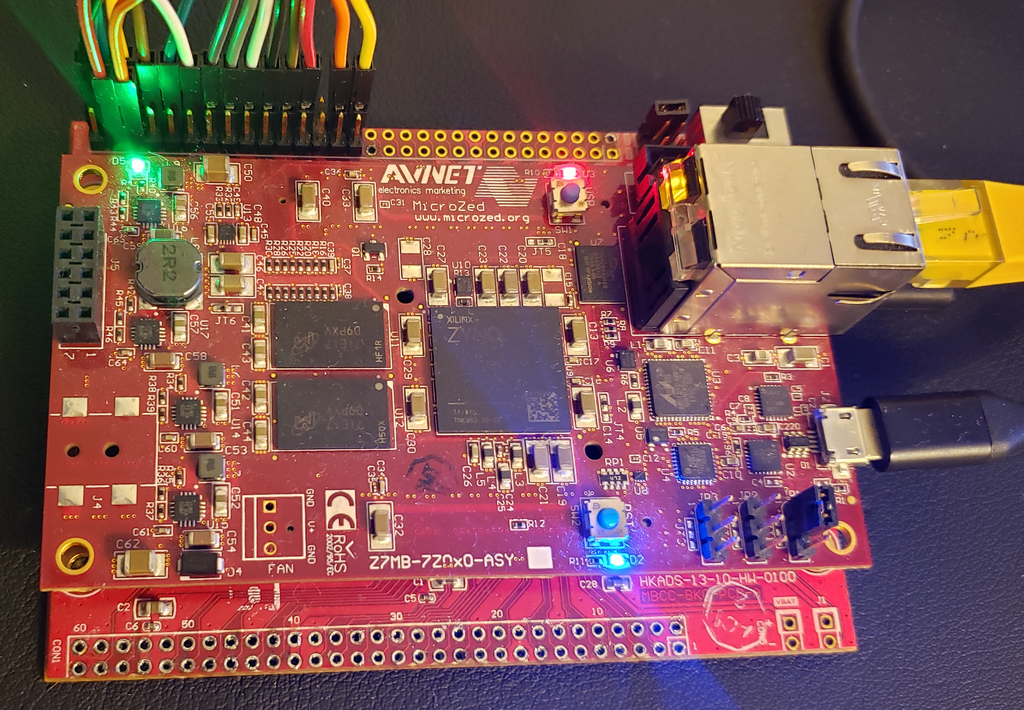
Following from the theory, the basic idea here is to digitize the voltage coming from some antenna, then use digital mixing with an oscillating signal of 60 kHz, and finally low pass filter the result to get the intensity of the WWVB broadcast. To do this digitally instead of analog, I’ll need to digitize the voltage at a much higher rate than the 60 kHz signal, so that I get a reasonable number of voltage points within each cycle. To do the mixing and filtering, I’ll need some fast logic, and an FPGA is the ideal choice.
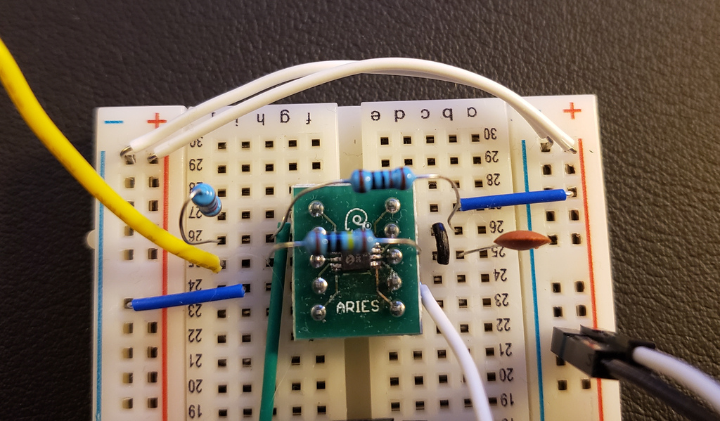
Analog front end amplifier
I opted to use a length of wire as an antenna, to start. This may seem a bit silly, but for an RF broadcast, a long length of wire can receive the oscillating electric field in the same way as any fancier antenna. More complicated designs tailor antennas to receive specific frequencies by matching the shape of the antenna to the physical shape of the RF wave. For 60 kHz, with a wavelength of around 5000 m, this isn’t very practical, and a long wire is quite optimal. Before trying to digitize the signal from the “antenna” it is necessary to match the voltage to the dynamic input range of the analog-to-digital converter (ADC). I’ll get to the details of the ADC in a bit, but suffice to say its input range is 0 to 2V, and provides a 1V reference for the mid point. The idea, then, is to bias the antenna to 1V, and let the received signals from the antenna cause this bias to fluctuate. These fluctuations will be very small, so amplifying them to larger values will improve the performance downstream, and put less stringent requirements on the ADC precision.

Fast analog-to-digital conversion
In a traditional heterodyne receiver, analog devices would be used to generate the oscillatory in-phase and quadrature signals, mix them, and perform low pass filtering. This was primarily done out of necessity, as until the last several decades, digital electronics were not fast and flexible enough to digitize and manipulate the RF directly. Direct conversion receivers, however, do just that.
The easiest operating mode for this ADC is to hold the conv signal high, and briefly lower it to trigger a conversion every 500 ns.
The eoc (end of conversion) will swing low when the conversion is complete.
The documentation suggested connecting this eoc signal to the pins for cs (channel select) and rd (read) if the ADC is being used stand-alone, such that the data appears out the output bus automatically when the conversion is completed.
A device (the FPGA in this project) can then latch the output data on the rising edge of eoc.
Some Verilog to do this follows, which includes a reset period to let the voltage references within the ADC stabilize, and a ready flag each for each clock sample that represents a new output value.
module adc_input(
    input clock,
    input reset,
    input [7:0] data_in,
    input eoc,
    output reg conv,
    output reg [7:0] data_out,
    output reg ready
    );

    reg [16:0] counter;
    reg initialized;

    initial
    begin
        counter = 0;
        initialized = 0;
        conv = 0;
        data_out = 0;
        ready = 0;
    end

    reg last_eoc;

    always @(posedge clock)
    begin
        if (reset)
        begin
            counter = 0;
            initialized = 0;
            conv = 0;
        end else
        begin
            if (eoc && !last_eoc)
            begin
                data_out = data_in;
                ready = 1;
            end else
            begin
                ready = 0;
            end
            last_eoc = eoc;
            counter = counter + 1;
            if (!initialized)
            begin
                if (counter == 3000) //30us with 100MHz clock
                begin
                    counter = 0;
                    initialized = 1;
                end
            end else
            begin
                if (counter == 50) //500ns with 100MHz clock
                begin
                    counter = 0;
                end
                conv = counter < 10 ? 0 : 1;
            end
        end
    end

endmodule
Software defined demodulation
With digitized data available in the FPGA, I just need to implement the signal generation of the in-phase and quadrature signals, mixing, and low pass filtering in Verilog. Generating a sine wave at a particular frequency is a bit of a trick in digital hardware. I opted for defining one cycle as counts of a 16 bit counter. One quarter of a sine wave is stored in a lookup table in the FPGA, since all four quarters are the same shape, just reversed in time, or inverted across zero. I only include 512 samples in this quarter, but this could be increased if more precision is required. Based on the high 2 bits of the counter, which divide the range into quarters, I can determine whether this quarter wave should be reversed or multiplied by , while using the next-lower 9 bits to determine the index of the lookup table. The remaining three bits allow for smaller increments of phase to be added in each clock cycle, to represent slower frequencies. More bits may be necessary, here, since my system clock runs at 100 MHz on the MicroZed.
In this way, a 16 bit signed decimal value can be returned that is proportional to the value of a sine wave at any phase. The cosine is just shifted by one quarter phase from the sine, so adding 1 to the top two bits of the phase allows the same trick to work. With an input clock and an adjustable phase increment per clock tick, output of many frequencies can be generated.
module sincos #(
    parameter FILE = "quarter_wave_512.hex"
)(
    input clock,
    input [15:0] phase_inc,
    output signed [15:0] sin,
    output signed [15:0] cos
);

    reg [15:0] phase;
    reg [15:0] lut[0:511];
    wire [1:0] quad;
    wire cos_quarter, sin_sign;
    wire cos_reverse, sin_reverse;
    wire [9:0] f_phase;
    wire [9:0] r_phase;

    assign quad = phase[15:14]+2'b1;
    assign sin_sign = phase[15];
    assign cos_sign = quad[1];
    assign sin_reverse = phase[14];
    assign cos_reverse = quad[0];
    assign f_phase = phase[13:5];
    assign r_phase = 511-phase[13:5];
    assign cos = cos_sign ? -lut[cos_reverse ? r_phase : f_phase] : lut[cos_reverse ? r_phase : f_phase];
    assign sin = sin_sign ? -lut[sin_reverse ? r_phase : f_phase] : lut[sin_reverse ? r_phase : f_phase];

    initial $readmemh(FILE, lut);
    initial phase = 0;

    always @(posedge clock)
    begin
        phase = phase + phase_inc;
    end

endmodule
Finally, the mixing and low-pass can be done, as a first pass, with a simple multiplication and integration.
In the following module, I’ve also included the ability to generate fake RF input that is a periodic chain of zeros and a carrier wave, to test the demodulation independent of the ADC input.
The ready flag from the ADC module is attached to the rf_clock input in the design for clocking data through the system.
As new down-sampled values are available, the valid flag will be asserted.
module sdr_receiver(
    input [7:0] rf_in,
    input [15:0] phase_inc,
    input [31:0] downsample_count,
    input use_fake,
    input [7:0] fake_log_period,
    input rf_clock,
    input clock,
    input reset,
    output valid,
    output reg signed [31:0] rf_downsample,
    output [31:0] carrier_strength,
    output signed [31:0] i_out,
    output signed [31:0] q_out
);

    reg [32:0] counter;
    always @(posedge clock)
    begin
        if (reset)
        begin
            counter = 0;
        end else
        begin
            counter = counter + 1;
        end
    end

    wire signed [15:0] cos;
    wire signed [15:0] sin;

    sincos quads(
        .clock(clock),
        .phase_inc(phase_inc),
        .cos(cos),
        .sin(sin)
    );

    wire signed [15:0] fake_carrier;
    sincos fakedata(
        .clock(clock),
        .phase_inc(phase_inc),
        .cos(fake_carrier),
        .sin()
    );
    wire signed [15:0] fake_rf = counter[fake_log_period]*fake_carrier ; //periodic carrier

    wire signed [7:0] data_in = use_fake ? fake_rf[15:8] : (rf_in-128);

    reg downsample_clock;
    reg [31:0] integral_count;
    reg signed [31:0] rf_integral;
    reg signed [31:0] rf_integral_cos;
    reg signed [31:0] rf_integral_sin;
    reg signed [31:0] mixed_cos_integral;
    reg signed [31:0] mixed_sin_integral;
    always @(posedge rf_clock)
    begin
        if (reset)
        begin
            downsample_clock = 0;
            integral_count = 0;
            rf_integral = 0;
            rf_integral_cos = 0;
            rf_integral_sin = 0;
            mixed_cos_integral = 0;
            mixed_sin_integral = 0;
        end else
        begin
            if (integral_count >= downsample_count)
            begin
                integral_count = 0;
                rf_downsample = rf_integral;
                mixed_cos_integral = rf_integral_cos;
                mixed_sin_integral = rf_integral_sin;
                downsample_clock = 1;
                rf_integral = 0;
                rf_integral_cos = 0;
                rf_integral_sin = 0;
            end else
            begin
                downsample_clock = 0;
                integral_count = integral_count + 1;
                rf_integral = rf_integral + data_in;
                rf_integral_cos = rf_integral_cos + cos*data_in;
                rf_integral_sin = rf_integral_sin + sin*data_in;
            end
        end
    end

    assign valid = downsample_clock;
    assign i_out = mixed_cos;
    assign q_out = mixed_sin;

    wire [63:0] power_sq = i_out*i_out + q_out*q_out;
    assign carrier_strength = sqrt(power_sq);

    function [31:0] sqrt;
        input [63:0] num;
        reg [63:0] a;
        reg [31:0] q;
        reg [33:0] left,right,r;
        integer i;
    begin
        //initialize all the variables.
        a = num;
        q = 0;
        i = 0;
        left = 0;   //input to adder/sub
        right = 0;  //input to adder/sub
        r = 0;  //remainder
        //run the calculations for 16 iterations.
        for(i=0;i<16;i=i+1) begin
            right = {q,r[33],1'b1};
            left = {r[31:0],a[63:62]};
            a = {a[61:0],2'b00};    //left shift by 2 bits.
            if (r[33] == 1) //add if r is negative
                r = left + right;
            else    //subtract if r is positive
                r = left - right;
            q = {q[30:0],!r[33]};
        end
        sqrt = q;   //final assignment of output.
    end
    endfunction //end of Function
Included here is a borrowed function for a clever way of computing the square root of an integer in Verilog.
Early results / next steps
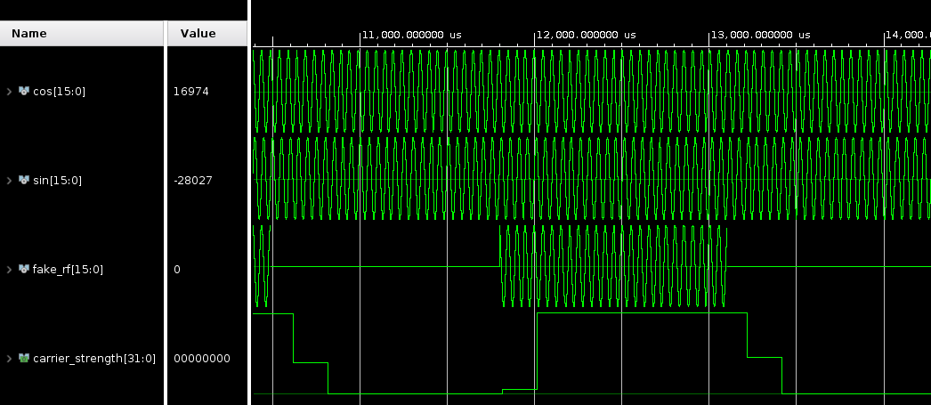
Simulating the modules above in fake data mode demonstrates that the general principle of the design works.
Shown below are the internally generated sine and cosine signals, the fake_rf signal, and the result of demodulation carrier_strength which shows a train of pulses, as expected.
I’ve generated a PetaLinux distribution for the ARM cores on my MicroZed, and a Vivado project including the Verilog above and some modules to generate an AXI device to control the configurable parameters as memory reads and writes from the Linux system.
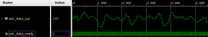
Using an integrated logic analyzer (ILA) added to the Vivado project, along with Xilinx’s virtual JTAG cable software, I can also verify that the ADC is digitizing what looks like RF signals from the antenna.
I’ll need to do some turning to get the generated waveforms to match 60 kHz, and actually start looking at the reception quality of 60 kHz signals.
All of this would be significantly easier with a decent oscilloscope, so perhaps I’ll see about acquiring one of those before going much further…
So, check back some time in the future for more info about actually receiving and decoding the WWVB time signal!
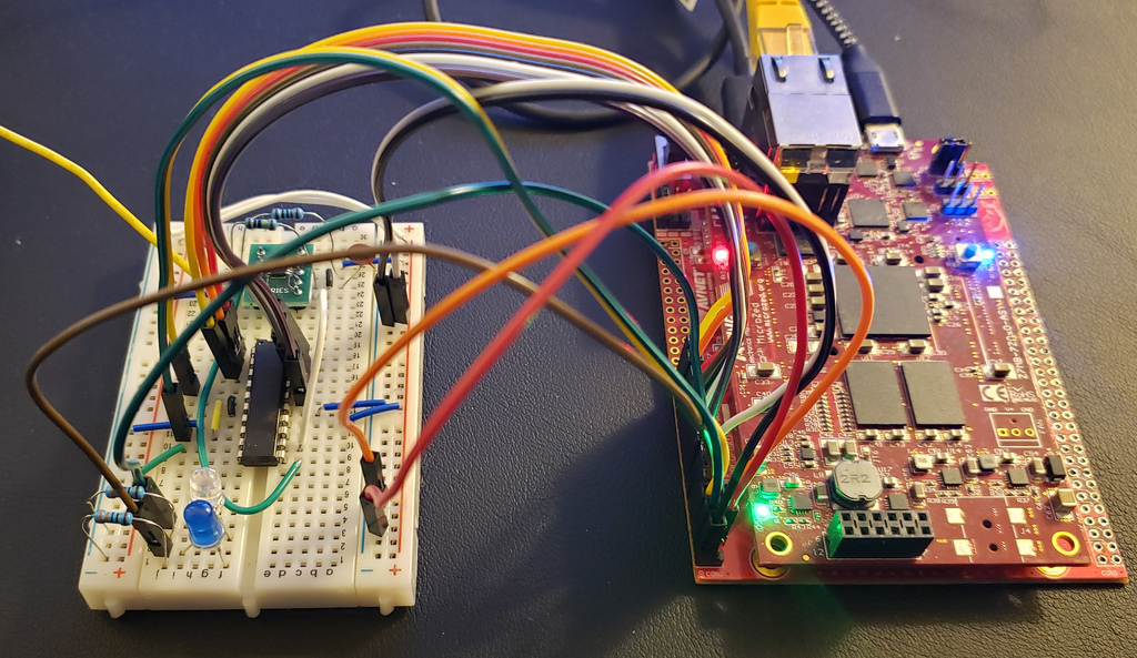
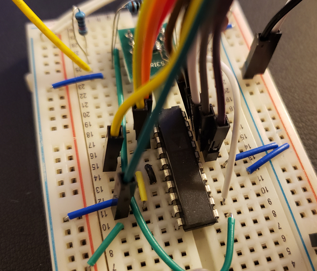
The current state of the WWVB direct conversion receiver. The “antenna” is the yellow wire going off to the left. Some status LEDs are included on the breadboard, with IO pins for selecting fake data mode, and performing a reset.